

|
| MOQ: | 10PCS |
| Price: | NEGOTIABLE |
| Standard Packaging: | 288PCS/TRAY |
| Delivery Period: | 2-3DAYS |
| Payment Method: | T/T |
| Supply Capacity: | 1360000pcsWEEK |
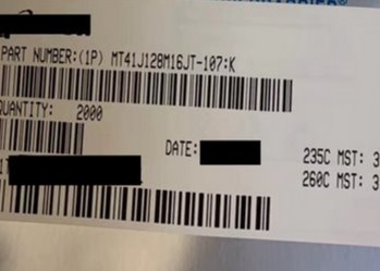
MT41J128M16JT-107:K DRAM 2G 128Mx16 DDR3Multipurpose register
1.Features
VDD = VDDQ = 1.5V ±0.075V
• 1.5V center-terminated push/pull I/O
• Differential bidirectional data strobe
•8n-bit prefetch architecture
• Differential clock inputs (CK, CK#)
• 8 internal banks
• Nominal and dynamic on-die termination (ODT)for data, strobe, and mask signals
• Programmable CAS READ latency (CL)
• Posted CAS additive latency (AL)
• Programmable CAS WRITE latency (CWL) based ontCK
• Fixed burst length (BL) of 8 and burst chop (BC) of 4(via the mode register set [MRS])
• Selectable BC4 or BL8 on-the-fly (OTF)
• Self refresh mode
•TC of 0°C to 95°C– 64ms, 8192 cycle refresh at 0°C to 85°C– 32ms, 8192 cycle refresh at 85°C to 95°C
• Self refresh temperature (SRT)
• Automatic self refresh (ASR
• Write leveling
• Multipurpose register
• Output driver calibration
2.Functional Description
DR3 SDRAM uses a double data rate architecture to achieve high-speed operation.The double data rate architecture is an 8n-prefetch architecture with an interface de-signed to transfer two data words per clock cycle at the I/O pins. A single read or writeoperation for the DDR3 SDRAM effectively consists of a single 8n-bit-wide, four-clock-cycle data transfer at the internal DRAM core and eight corresponding n-bit-wide, one-half-clock-cycle data transfers at the I/O pins.The differential data strobe (DQS, DQS#) is transmitted externally, along with data, foruse in data capture at the DDR3 SDRAM input receiver. DQS is center-aligned with datafor WRITEs. The read data is transmitted by the DDR3 SDRAM and edge-aligned to thedata strobes.The DDR3 SDRAM operates from a differential clock (CK and CK#). The crossing of CKgoing HIGH and CK# going LOW is referred to as the positive edge of CK. Control, com-mand, and address signals are registered at every positive edge of CK. Input data is reg-istered on the first rising edge of DQS after the WRITE preamble, and output data is ref-erenced on the first rising edge of DQS after the READ preamble.Read and write accesses to the DDR3 SDRAM are burst-oriented. Accesses start at a se-lected location and continue for a programmed number of locations in a programmedsequence. Accesses begin with the registration of an ACTIVATE command, which is thenfollowed by a READ or WRITE command. The address bits registered coincident withthe ACTIVATE command are used to select the bank and row to be accessed. The ad-dress bits registered coincident with the READ or WRITE commands are used to selectthe bank and the starting column location for the burst access.The device uses a READ and WRITE BL8 and BC4. An auto precharge function may beenabled to provide a self-timed row precharge that is initiated at the end of the burstaccess.As with standard DDR SDRAM, the pipelined, multibank architecture of DDR3 SDRAMallows for concurrent operation, thereby providing high bandwidth by hiding row pre-charge and activation time.A self refresh mode is provided, along with a power-saving, power-down mode.
3.Functional Block Diagrams
DDR3 SDRAM is a high-speed, CMOS dynamic random access memory. It is internallyconfigured as an 8-bank DRAM
![]()
4.Why choose us?
100% new and originao with Advantage price
High efficiency
Fast Delivery
Professional team service
10 Years Experience Electronic components
Electronic components Agent
Advantage logistic discount
Excellent After-sales Service
|
|
| MOQ: | 10PCS |
| Price: | NEGOTIABLE |
| Standard Packaging: | 288PCS/TRAY |
| Delivery Period: | 2-3DAYS |
| Payment Method: | T/T |
| Supply Capacity: | 1360000pcsWEEK |
MT41J128M16JT-107:K DRAM 2G 128Mx16 DDR3Multipurpose register
1.Features
VDD = VDDQ = 1.5V ±0.075V
• 1.5V center-terminated push/pull I/O
• Differential bidirectional data strobe
•8n-bit prefetch architecture
• Differential clock inputs (CK, CK#)
• 8 internal banks
• Nominal and dynamic on-die termination (ODT)for data, strobe, and mask signals
• Programmable CAS READ latency (CL)
• Posted CAS additive latency (AL)
• Programmable CAS WRITE latency (CWL) based ontCK
• Fixed burst length (BL) of 8 and burst chop (BC) of 4(via the mode register set [MRS])
• Selectable BC4 or BL8 on-the-fly (OTF)
• Self refresh mode
•TC of 0°C to 95°C– 64ms, 8192 cycle refresh at 0°C to 85°C– 32ms, 8192 cycle refresh at 85°C to 95°C
• Self refresh temperature (SRT)
• Automatic self refresh (ASR
• Write leveling
• Multipurpose register
• Output driver calibration
2.Functional Description
DR3 SDRAM uses a double data rate architecture to achieve high-speed operation.The double data rate architecture is an 8n-prefetch architecture with an interface de-signed to transfer two data words per clock cycle at the I/O pins. A single read or writeoperation for the DDR3 SDRAM effectively consists of a single 8n-bit-wide, four-clock-cycle data transfer at the internal DRAM core and eight corresponding n-bit-wide, one-half-clock-cycle data transfers at the I/O pins.The differential data strobe (DQS, DQS#) is transmitted externally, along with data, foruse in data capture at the DDR3 SDRAM input receiver. DQS is center-aligned with datafor WRITEs. The read data is transmitted by the DDR3 SDRAM and edge-aligned to thedata strobes.The DDR3 SDRAM operates from a differential clock (CK and CK#). The crossing of CKgoing HIGH and CK# going LOW is referred to as the positive edge of CK. Control, com-mand, and address signals are registered at every positive edge of CK. Input data is reg-istered on the first rising edge of DQS after the WRITE preamble, and output data is ref-erenced on the first rising edge of DQS after the READ preamble.Read and write accesses to the DDR3 SDRAM are burst-oriented. Accesses start at a se-lected location and continue for a programmed number of locations in a programmedsequence. Accesses begin with the registration of an ACTIVATE command, which is thenfollowed by a READ or WRITE command. The address bits registered coincident withthe ACTIVATE command are used to select the bank and row to be accessed. The ad-dress bits registered coincident with the READ or WRITE commands are used to selectthe bank and the starting column location for the burst access.The device uses a READ and WRITE BL8 and BC4. An auto precharge function may beenabled to provide a self-timed row precharge that is initiated at the end of the burstaccess.As with standard DDR SDRAM, the pipelined, multibank architecture of DDR3 SDRAMallows for concurrent operation, thereby providing high bandwidth by hiding row pre-charge and activation time.A self refresh mode is provided, along with a power-saving, power-down mode.
3.Functional Block Diagrams
DDR3 SDRAM is a high-speed, CMOS dynamic random access memory. It is internallyconfigured as an 8-bank DRAM
![]()
4.Why choose us?
100% new and originao with Advantage price
High efficiency
Fast Delivery
Professional team service
10 Years Experience Electronic components
Electronic components Agent
Advantage logistic discount
Excellent After-sales Service

